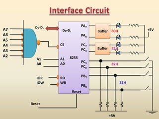
10+ 8255 block diagram
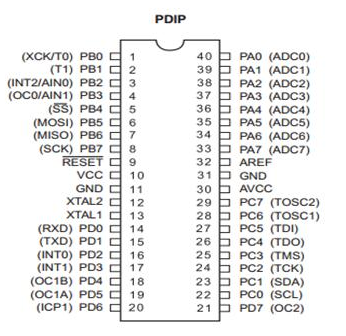
2 Pin Diagram of 8255. The signal description of 8255 are briefly presented as follows.
Atmega32 Pin Diagram Javatpoint
Data busD 0 -D 7.

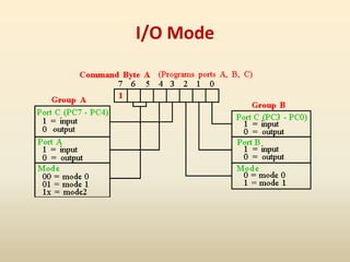
. There are two different modes of 8255. These are 8 -bit bi-directional buses connected to 8085 data bus for transferring data. Bit Set Reset BSR Mode.
The 8085 activates the WR input of 8255 when it wants to write data to a port of 8255. It is connected to WR output of 8085. The block diagram of 8255 is like this.
These are eight port A lines that acts as either latched output or buffered input lines. Programmable Peripheral Interface Block Diagram. Describe the Block diagram of 8255.
Bit Set Reset BSR Mode. It is an active low input pin for 8255.
Intel 8080 Wikiwand
2
2
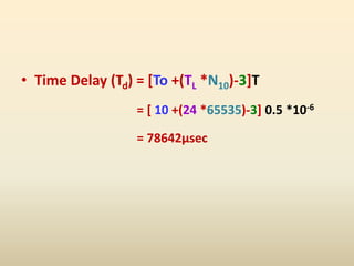
8255 Programming
2
2
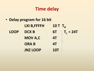
8255 Programming

2019 2 3l Ecoboost Water Pump Housing Part Number Ford Mustang Ecoboost Forum
8255 Programming
8255 Programming
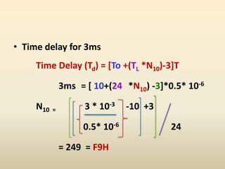
8255 Programming

8255 Programming

Control System In Mechatronics Open Loop Closed Loop Control System Mechatronics Control Variable Control System
Atmega32 Pin Diagram Javatpoint
How Does Computer Hardware And Software Work Together To Process Information Quora
What Are Some Good Books On Microcontrollers And Microprocessers Quora
Keyboard Interfacing With Avr Javatpoint